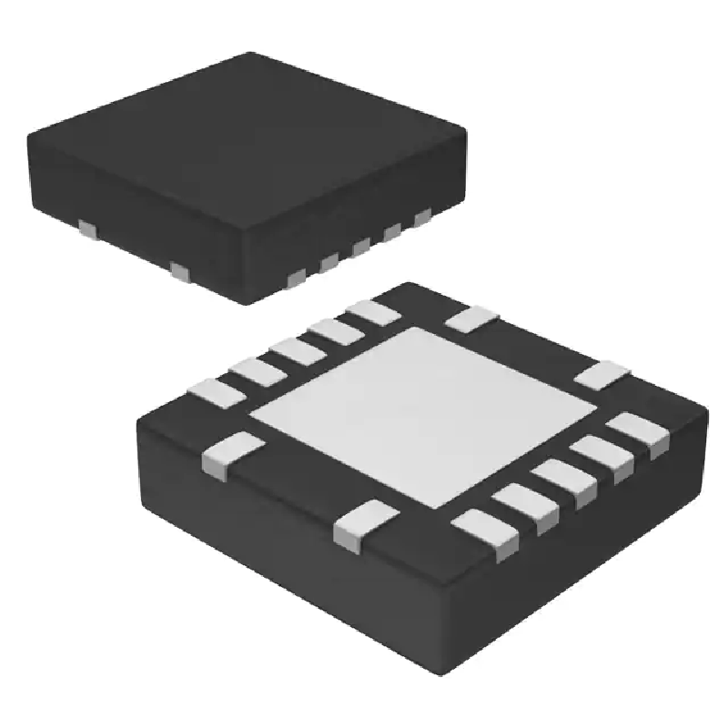
TPS54620RGYR
Features
1.Integrated 26 mΩ and 19 mΩ MOSFETs
2.Split Power Rail: 1.6 V to 17 V on PVIN
3.200-kHz to 1.6-MHz Switching Frequency
4.Synchronizes to External Clock
5.0.8 V ±1% Voltage Reference Overtemperature
6.Low 2-µA Shutdown Quiescent Current
7.Monotonic Start-Up into Prebiased Outputs
8.–40°C to 150°C Operating Junction Temperature
Range
1.Adjustable Slow Start and Power Sequencing
2.Power Good Output Monitor for Undervoltage and
Overvoltage Monitoring
Adjustable Input Undervoltage Lockout
For SWIFT™ Documentation, Visit
http://www.ti.com/swift
Create a Custom Design Using the TPS54620
With the WEBENCH Power Designer
Applications
1.High Density Distributed Power Systems
2.High Performance Point of Load Regulation
3.Broadband, Networking and Optical
Communications Infrastructure Description The TPS54620 in thermally enhanced 3.50 mm ×
3.50 mm QFN package is a full featured 17-V, 6-A,synchronous, step-down converter which is optimized for small designs through high efficiency and integrating the high-side and low-side MOSFETs.Further space savings are achieved through current mode control, which reduces component count, and by selecting a high switching frequency, reducing the footprint of the inductor.The output voltage start-up ramp is controlled by the SS/TR pin which allows operation as either a standalone power supply or in tracking situations. Power sequencing is also possible by correctly configuring the enable and the open-drain power good pins. Cycle-by-cycle current limiting on the high-side FET protects the device in overload situations and is enhanced by a low-side sourcing current limit which prevents current runaway. There is also a low-side sinking current limit that turns off the low-side MOSFET to prevent excessive reverse current. Thermal shutdown disables the part when die temperature exceeds thermal shutdown temperature.
Device Information
PART NUMBER PACKAGE BODY SIZE (NOM)
TPS54620 VQFN (14) 3.50 mm × 3.50 mm


